

Electroless Nickel and Immersion Gold
Flat solderable surface allows tighter placement of surface mount pads
Finish is bondable with aluminum wire
Electroless Nickel and Immersion Gold, applicable specification - IPC-4552
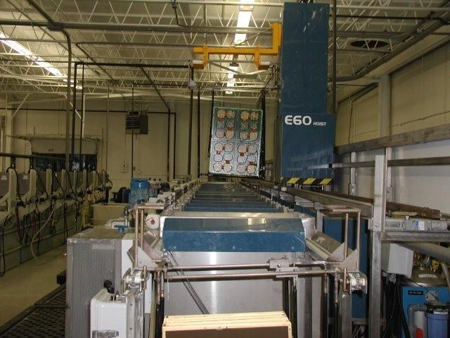
Electroless Nickel / Immersion Gold is a final finish offered by Alternate Finishing for printed circuit boards with surface mount technology (SMT) and ball grid array (BGA) designs. The process line is fully automated with vibration in all of the process stations to make sure bubbles are removed from the holes.
Electroless Nickel metallization is applied after copper trace/feature definition (after Cu plate, image and etch operations). It can be applied before or after soldermask application. It provides a conformal coating on all exposed copper surfaces including sidewalls.
It uses a special process in chemical processing tanks to chemically deposit a nominal 120 - 240 micro-inches of approximately 93% purity nickel over exposed copper traces and features. Intrinsic to the electroless process is a significant amount of phosphorous ( 6 to 8%) that is co-deposited with the nickel.
The nickel acts as barrier layer between the copper and the gold, preventing unwanted (unsolderable) intermetallic formation. The nickel layer also adds strength to plated through holes and vias. The hardness of the nickel also increases wear resistance.
Immersion Gold is applied after the electroless nickel process. It also provides a gold coating on all exposed nickel surfaces including sidewalls.
It is a molecular replacement process in which previously deposited nickel molecules are replaced by gold molecules in a processing tank. The gold deposited is 99.99% pure, and its thickness is allowed to build up to 3 to 8 micro-inches. By design the immersion deposition process is self limiting. When the underlying nickel is completely covered the reaction will stop and no more gold will deposit. Immersion gold provides excellent solderability properties, and it retards passivation (oxidation) of the nickel layer.
The combined nickel/gold metallization provides excellent corrosion resistance, solderabilty, pad coplanarity and shelf life. It is a good choice for fine-pitch SMT and BGA technologies.
Recommendations
Size limits - The size most often received is 24" x18" but panels can be any size up to 26" x 30"
The service we provide can be applied to your parts in one of the following ways.
We can plate the whole panel after you etch it. No tin or tin-lead may be exposed anywhere on the panel including edges and inside holes. We recommend that you run the panels through the solder strip with some extra time to ensure all the intermettalic layer is removed and that you bake the panels at 250 deg F for one hour.
We can plate the pads only. This is done after you apply the solder mask on the bare copper. If holes are plugged they need to be completely plugged flush. Holes that are partially filled with solder mask or plugged from one side cause incomplete catalysation and some pads may not plate correctly.
We plate panels that have many different brands of solder mask and do not recommend any particular brand or model. However, please follow closely any recommendations that your mask supplier has regarding preparing panels for electroless nickel and immersion gold plating. General recommendations to ensure adequate solder mask adhesion are:
It is very important that the tin or tin-lead used for etch resist is completely removed prior to soldermask application.
Avoid tight registration of the solder mask. If possible open a window around rows of fine pitched features.
Solder mask must be fully cured however, take care not to over cure it.
Boards must stabilize after processing. Panels that fail soldermask adhesion tests after processing will likely pass in as little as a few hours or the next day. For this reason we only tape test on waste areas of the panel for plating adhesion tests.
For more information on any of our services, please feel free to contact us.